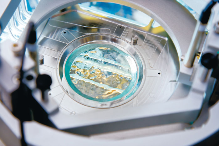
Today’s semiconductor manufacturing uses Photolithography in the microfabrication process to pattern parts of a thin film or the bulk of a substrate. It uses extreme ultra violet light to transfer complex geometric patterns from a photomask to a light-sensitive chemical “photoresist” on the substrate. A series of chemical treatments then either engraves the exposure pattern into, or enables deposition of a new material in the desired pattern upon, the material underneath the photo resist.
The complex optical systems used in lithography systems are critical to shrinking the size of microchips. One way to pack more, smaller circuits onto a semiconductor is to use light with a shorter wavelength, such as ultra-violet light. At such narrow wavelengths, regular air would distort the beam path and that is why they are often operated in atmospheres of hydrogen or other gas blends.
When hydrogen atmospheres are used for lithography optics, that hydrogen must be very pure. For monitoring and validating hydrogen quality, engineers can use the parts-per-billion levels of detection found in the HEMS analyzer. The HEMS instrument can continuously sample the hydrogen quality directly from feed lines, eliminating the need for offline measurements performed by scientists in a laboratory.
Photolithography
shares some fundamental principles with photography in that the pattern in the etching resist is created by exposing it to light, either directly (without using a mask) or with a projected image using an optical mask. This procedure is comparable to a high precision version of the method used to make printed circuit boards. Subsequent stages in the process have more in common with etching than with lithographic printing. It is used because it can create extremely small patterns (down to a few tens of nanometers in size), it affords exact control over the shape and size of the objects it creates, and because it can create patterns over an entire surface cost-effectively. Its main disadvantages are that it requires a flat substrate to start with, it is not very effective at creating shapes that are not flat, and it can require extremely clean operating conditions.
